Routage Pcb

Routage D Un Pcb Avec Kicad Devenez Pro En Electronique
7 Raisons De Concevoir Vos Cartes Electroniques Avec Solidworks Pcb Visiativ Solutions

Du Schema Au Routage Des Cartes Electroniques Bonnes Pratiques Application Au Design De Pcb Sous Kicad Eda Captronic
Pcb Avec Kicad
Contact Routagepcb Fr Routage De Circuit Imprime 77

Typon Routage De Carte Electronique Sous Ares Simple Face A Strap Youtube
PCB Layout Make professional PCB layouts with up to 32 copper layers KiCad now has a push and shove router which is capable of routing differential pairs and interactively tuning trace lengths Learn more 3D Viewer KiCad includes a 3D viewer which you can use to inspect your design in an interactive canvas You can rotate and pan around to.

Routage pcb. Routing, the process of connecting all the pads of a printed circuit board (PCB) layout, can be a timeconsuming and tedious process To avoid the time and frustration of manually routing your PCB, there are various software tools called autorouters which can do this for you. At the PCB, the USB connector consists of 4 main signals VBUS (5V power), Ground and USB DP and DM DP and DM are the differential pair As with twisted pair cabling, these two signals must be closely matched with the following characteristics Equal length Both DP and DM signals must travel the same distance If one trace ends up. PCB Layout Make professional PCB layouts with up to 32 copper layers KiCad now has a push and shove router which is capable of routing differential pairs and interactively tuning trace lengths.
Can be very useful when component cost or PCB area is of concern This document will explain how to connect the USB pins of an EFM32 microcontroller, and will give general guidelines on PCB design for USB applications First some quick rulesofthumb for routing and layout are presented before a more detailed explanation follows. Routage pcb, pcb routing, circuits imprimés, printed circuits, schématique. Create a chassis ground ring connecting the entire perime ter of the PCB The purpose of this is to improve ESD performance and help reduce radiated emissions The chassis ground ring should be a minimum of 127 mm (50 mils) wide, if pos sible, and be routed on all layers with the rings stitched together with GND vias.
Le routage est un processus qui permet de sélectionner des chemins dans un réseau pour transmettre des données depuis un expéditeur jusqu'à un ou plusieurs destinataires On parle de routage. In electronic design, wire routing, commonly called simply routing, is a step in the design of printed circuit boards (PCBs) and integrated circuits (ICs) It builds on a preceding step, called placement, which determines the location of each active element of an IC or component on a PCB. The Saturn PCB Toolkit is the best freeware resource for PCB related calculations you can find It incorporates many features that PCB designers and engineers are in regular need of like current capacity of a PCB trace, via current, differential pairs and much more Please download our PCB Toolkit today for free and enjoy!.
Open your PCB layout (brd) file from your Autodesk EAGLE Control Panel Select the Autorouter tool on the lefthand side of your interface to open the Autorouter Main Setup dialog You’re in complete control of the autorouter setup with settings for effort, CPU threads, and routing directions. This application report can help system designers implement best practices and understand PCB layout options when designing platforms This document is intended for audiences familiar with PCB manufacturing, layout, and design 12 Critical Signals A primary concern when designing a system is accommodating and isolating highspeed signals As high. The copper in a PCB is rated in ounces, and represents the thickness of 1 ounce of copper rolled out to an area of 1 square foot Table 1 shows a listing of the PCB copper thickness relative to its rating Reproduced from Daycounter Engineering Services Web site For example, a PCB rated at 1 oz copper has a copper thickness of 34 µm (").
Such boards cost at least twice as much in these quantities, and the 2layer PCB still costs more than the components combined. To avoid the risk of accidental short circuits, I prefer not to push the PCB manufacturing limits except in those few areas of the board where there’s no alternative A good example is autorouting between adjacent pins of a 01 inch header There’s roughly 30 mils of space between the metal rings that surround adjacent pins, providing. Keep the PHY device and the differential transmit pairs at least 25mm (approx 1 inch) from the edge of the PCB, up to the magnetics If the magnetics are integrated into the RJ45, the differential pairs should be routed to the back of the integrated magnetics RJ45 connector, away from the board edge.
PCB Classification “Pattern and Drill Specification” are used shorthandly to measure the manufacturability of the PCB this generate a classification which is related to the PCBoard’s Services Any way these classes generally permit to control the price of the PCB on demand service. Layers Overview PCB composition is all about layering one material over another The thickest, middle part of the board is a insulating substrate (usually FR4)On either side of that is a thin layer of copper, where our electric signals pass throughTo insulate and protect the copper layers, we cover them with a thin layer of lacquerlike soldermask, which is what gives the PCB color (green. Making the physical board is a different task, and there are a lot of tutorials on the net (and even some instructables) on making the board after you have the design.
Size decreases, the challenges for PCB routing increase as there is less room to route traces and vias between package balls This guide illus trates various methods for successful design regardless of pitch size Note Throughout this guide, various specifications and estimates are given regarding PCB pricing, costs, and technology. Technicien Etudes Routage PCB H/F étape 1 Votre profil (CV et LM) étape 2 Compléments d'information étape 3 Questionnaire X Les données personnelles collectées par le biais de ce formulaire font l’objet d’un traitement de la part de notre société aux fins d’étudier votre candidature Nous vous informons que les données vous. Nous réalisons toute la phase de conception électronique d’un produit ou d’un système électronique embarqué étude de faisabilité et élaboration des schémas électroniques, CAO électronique du circuit imprimé (routage PCB) et fabrication de la carte électronique.
Site de routage de circuit imprime 77 Du routage de carte à la gestion complète d'une étude en passant par le développement de moyens (simulateurs HIL, Firmwares, programmes sur PC etc), RoutagePCBfr propose tous les services associés au développement d'une carte électronique en un délai record. Le routage est un processus qui permet de sélectionner des chemins dans un réseau pour transmettre des données depuis un expéditeur jusqu'à un ou plusieurs destinataires On parle de routage. Routage de sortance BGA January 6, Download PDF Download the PDF to keep learning offline Download PDF Developing a PCB Testing Procedure For New Designs Before your new device comes off the fabrication line, it will need to go through a comprehensive PCB testing procedure Here’s how to create a PCB testing procedure for new boards.
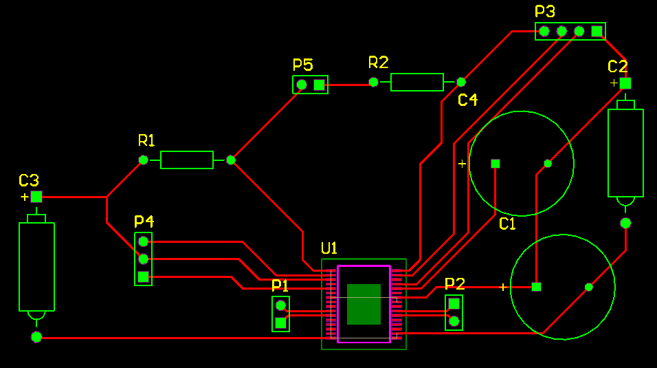
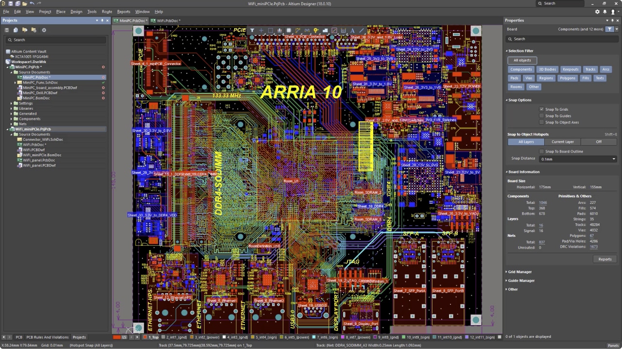
Routage PCB Vérification routage (DRC) Fichier de sortie Document de schématique Document de routage Figure 2 – Flot de conception d’un circuit imprimé (PCB) Ces 2 documents sont liés A chaque composant électronique, on associe un symbole électrique et. Cours Informatique Réseaux Informatiques ajouté le 18/11/17 ra consacré aux appareils et les techniques d’interconnexion niveau 1 et 2 tel que les répéteurs, les hubsrépéteurs, les ponts et les méthodes de pontage, les routeurs et les protocoles de routageFinalement on traite les protocoles de base TCP IP introduction aux reseaux locaux La norme 8023 – les reseaux. The PCB stackup design plays a central part in the overall system performance, especially with highperformance FPGAs that incorporate transceiver technology The PCB stackup is the substrate upon which all design components are assembled A poorly designed PCB stackup with inappropriately selected materials can degrade the.
Quelques règles de routage PCB pour une faible publicité INSTITUT NATIONAL DES SCIENCES APPLIQUEES DE and on Devices – Limits and Methods of Measurement », August 02 Montrose 1996 M I Montrose, “Printed Circuit Board Design Techniques for EMC Compliance”, IEEE Press, 1996, ISBN Dunand 00 P Dunand. PCB design guidelines state good power supply in a PCB layout equates to the distribution of your power supply signal(s) This often is designed as a copper power plane that reaches all required devices, components, and circuits within an acceptable range or level that allows for desired operation. Prior to working in the PCB industry, he taught at Portland State University He conducted his Physics MS research on chemisorptive gas sensors and his Applied Physics PhD research on random laser theory and stability His background in scientific research spans topics in nanoparticle lasers, electronic and optoelectronic semiconductor.
The Saturn PCB Toolkit is the best freeware resource for PCB related calculations you can find It incorporates many features that PCB designers and engineers are in regular need of like current capacity of a PCB trace, via current, differential pairs and much more. Place and route is a stage in the design of printed circuit boards, integrated circuits, and fieldprogrammable gate arrays As implied by the name, it is composed of two steps, placement and routing. Going 4layer is acceptable only if TRULY necessary;.
Routage pcb, pcb routing, circuits imprimés, printed circuits, schématique. Going 4layer is acceptable only if TRULY necessary;. The copper in a PCB is rated in ounces, and represents the thickness of 1 ounce of copper rolled out to an area of 1 square foot Table 1 shows a listing of the PCB copper thickness relative to its rating Reproduced from Daycounter Engineering Services Web site For example, a PCB rated at 1 oz copper has a copper thickness of 34 µm (").
An engineer must order a minimum of 10 to boards and wait ONE to TWO weeks in order to receive an initial PCB prototype Usually, the prototype is populated with components and then tested If the test results are unfavorable or the engineer wants to test a second iteration, then the design has to be reconfigured and a set of prototypes created a second time, usually taking another ONE to. Long distance traces should be routed at an offangle to the XY axis of a PCB layer, in order to distribute the effects of fiberglass bundle weaves and resinrich areas of the dielectric. This tutorial discusses proper printedcircuit board (PCB) grounding for mixedsignal designs For most applications a simple method without cuts in the ground plane allows for successful PCB layouts with this kind of IC Next, we learn how to place components and route signal traces to minimize problems with crosstalk.
In a previous Instructable, I provided an intro to schematic entry using CadSoft's EAGLE editor In this instructable, we'll make a printed circuit board from that schematic I guess I should say that we'll make a PCB DESIGN;. Size decreases, the challenges for PCB routing increase as there is less room to route traces and vias between package balls This guide illus trates various methods for successful design regardless of pitch size Note Throughout this guide, various specifications and estimates are given regarding PCB pricing, costs, and technology. The PCB stackup design plays a central part in the overall system performance, especially with highperformance FPGAs that incorporate transceiver technology The PCB stackup is the substrate upon which all design components are assembled A poorly designed PCB stackup with inappropriately selected materials can degrade the.
4/Soigner le routage des condensateurs de découplages en réduisant au maximum la surface décrite par les raccordements du condensateur aux liaisons alim, ainsi que les longueurs des fils En clair dans le cas d'un simple face, les 2 fils seront amenés en parallèle avec un faible écart entre eux. 2 PCB StackUp and Board Layout • At minimum, select a PCB with at least four layers Two layers are for signals while the remaining two are for power and ground • Use dedicated ground and power planes – Power and ground planes make an excellent highfrequency capacitor and act as an additional. First off This is for a oneoff (or twooff) hobby project, nothing more serious If this were a commercial design, I would go 4layer at once (though I wouldn't be designing such a project in the first place);.
At the PCB, the USB connector consists of 4 main signals VBUS (5V power), Ground and USB DP and DM DP and DM are the differential pair As with twisted pair cabling, these two signals must be closely matched with the following characteristics Equal length Both DP and DM signals must travel the same distance If one trace ends up. Le routage des circuits imprimés (ou Printed Circuit Board) réside d'une part à placer les composants sur le circuit et d'autre part à relier les différents composants entre eux par des. Such boards cost at least twice as much in these quantities, and the 2layer PCB still costs more than the components combined.
General PCB Guidelines This section lists general PCB layout and supply voltage guidelines The commonly used FR4 material works we ll for low frequency (500 to 600 MHz) applications GTEK or Teflon can be considered for highspeed designs Estimate the number, value, and type of decoupling capacitors required to develop. Browse other questions tagged pcb pcbdesign cadence allegro or ask your own question The Overflow Blog Podcast 284 pros and cons of the SPA The Overflow #46 What does it mean to be a productled company Featured on Meta Creating new Help Center documents for Review queues Project overview. Autodesk EAGLE is a powerful PCB design & schematic software for professional electronics designers, with easytouse schematic editor, and powerful PCB layout Worldwide Sites You have been detected as being from Where applicable, you can see countryspecific product information, offers, and pricing.
Site de routage de circuit imprime 77 Du routage de carte à la gestion complète d'une étude en passant par le développement de moyens (simulateurs HIL, Firmwares, programmes sur PC etc), RoutagePCBfr propose tous les services associés au développement d'une carte électronique en un délai record. 4/Soigner le routage des condensateurs de découplages en réduisant au maximum la surface décrite par les raccordements du condensateur aux liaisons alim, ainsi que les longueurs des fils En clair dans le cas d'un simple face, les 2 fils seront amenés en parallèle avec un faible écart entre eux. PCB Classification “Pattern and Drill Specification” are used shorthandly to measure the manufacturability of the PCB this generate a classification which is related to the PCBoard’s Services Any way these classes generally permit to control the price of the PCB on demand service.
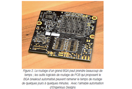
Your choice for BGA routing may significantly affect the signal integrity and manufacturability of your PCB design Additionally, your selection may add days to your board’s turnaround time By implementing BGA routing guidelines and best practices, you can ensure the manufacturability of your board and reduce build time for your PCB. Can be very useful when component cost or PCB area is of concern This document will explain how to connect the USB pins of an EFM32 microcontroller, and will give general guidelines on PCB design for USB applications First some quick rulesofthumb for routing and layout are presented before a more detailed explanation follows. PCB Layout Recommendations for BGA Packages Technical Note FPGATN October.
Routing, the process of connecting all the pads of a printed circuit board (PCB) layout, can be a timeconsuming and tedious process To avoid the time and frustration of manually routing your PCB, there are various software tools called autorouters which can do this for you. 1 Efficient use of PCB space Using BGA packages means fewer component involvement and smaller footprints, it is also help to save space for custom PCBs, which greatly increases the effectiveness of PCB space 2 Improve thermal and electrical performance Due to small size of PCB base on BGA package, heat dissipation is more easily. There’s an old saying that goes something like this – PCB design is 90% placement and 10% routing This is still true today, and the placement of your components will end up deciding how much time your routing will take, but that doesn’t mean that routing your PCB is any less important.
Dans tout système électronique, le routage PCB est un paramètre indispensable pour garantir une communication plus aisée Le routage PCB s’occupe d’un nombre important de données transmises sur un réseau électronique Il est un système qui permet de connecter les composants électriques entre eux. Panasonic Electronic Materials, Product information site of Printed Circuit Board Materials (Copper Clad Laminates), Semiconductor Encapsulation Materials, Adhesive, Plastic Molding Compounds and Advanced Films for various application Automotive components, ICT infrastructure equipment, Mobile products, IC Package, LED, Appliances, Amusement, etc. Starting a new PCB, Doing Layout, Layer Sets, DRC CheckStepbyStep video for everyone starting with Altium Designer PCB Layout and Schematic Enjoy )Links.
First off This is for a oneoff (or twooff) hobby project, nothing more serious If this were a commercial design, I would go 4layer at once (though I wouldn't be designing such a project in the first place);. To avoid the risk of accidental short circuits, I prefer not to push the PCB manufacturing limits except in those few areas of the board where there’s no alternative A good example is autorouting between adjacent pins of a 01 inch header There’s roughly 30 mils of space between the metal rings that surround adjacent pins, providing. In this course, you learn how to use the Allegro ® PCB Router to perform automatic and interactive routing You run autorouting, modify design rules, run interactive routing, analyze router log files, fan out a design, and improve manufacturability You also restrict routing to specific areas of the board and keep signals away from other areas.
Prior to working in the PCB industry, he taught at Portland State University He conducted his Physics MS research on chemisorptive gas sensors and his Applied Physics PhD research on random laser theory and stability His background in scientific research spans topics in nanoparticle lasers, electronic and optoelectronic semiconductor.

Editeur De Pcb Outil De Mise En Page Ecadstar
Pdn De Pcb Analyse Et Modelisation Altium
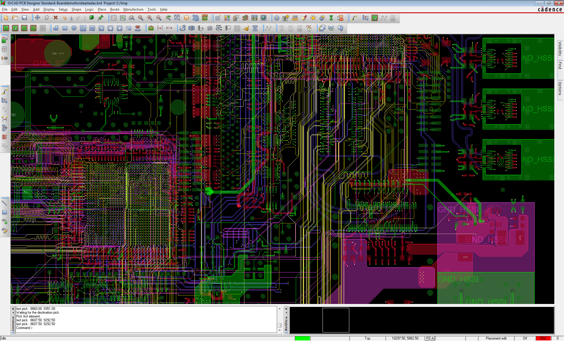
Orcad Pcb Designer Suite
Q Tbn And9gctbgfjwplss0vgfre P8xfihgv5jvkylbw2 Ujfd3c2513ha6k0 Usqp Cau
Guide De Routage Ruban Vs Microruban Blog Altium Designer
Assemblage De Circuit Imprime Conception Electronique Routage De Pcb A Montreal Quebec
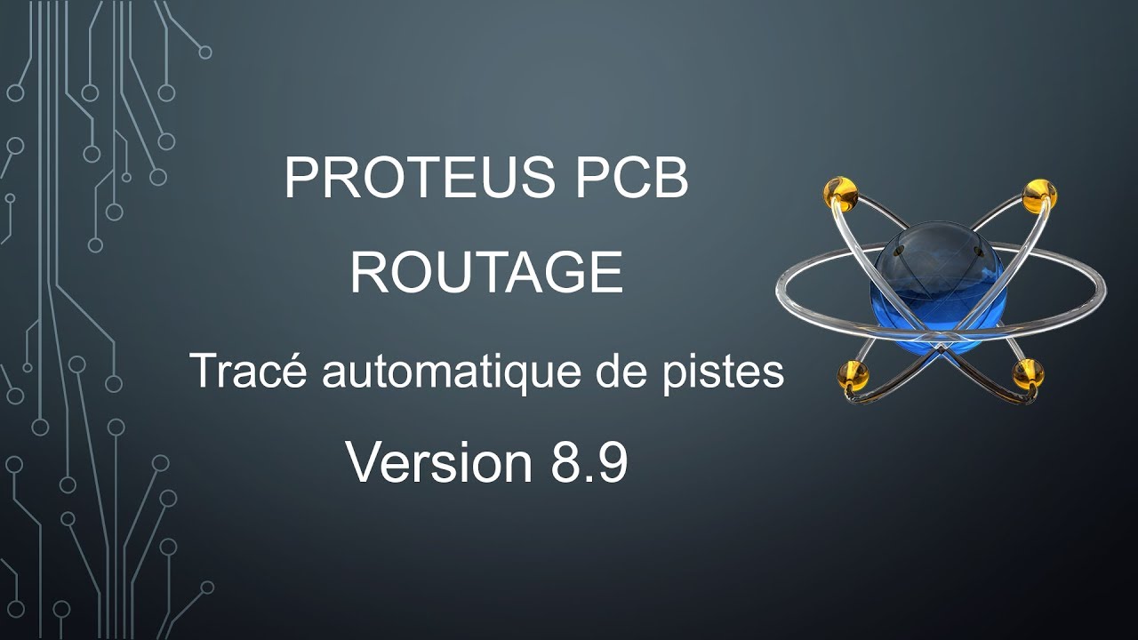
Proteus V8 Pcb Routage Trace Automatique De Piste Multipower Education Pros Youtube
Pcb Layout Diptrace
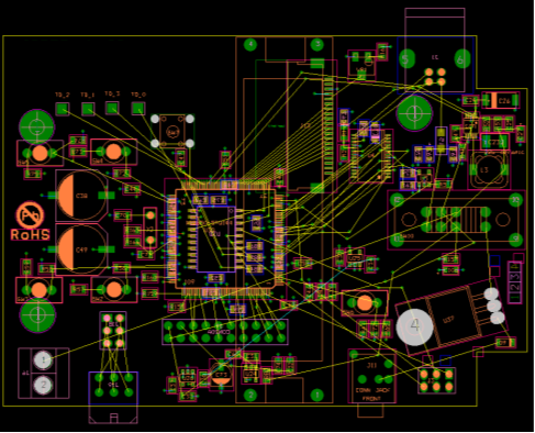
Maitrisez La Schematique Et Le Routage Concevez Un Objet Connecte Autonome Du Capteur A Son Antenne Openclassrooms
Q Tbn And9gcsekwurzktfjtlubptmxt Imiz1rkzufqr1pfv Tzhrzzhbvqeh Usqp Cau

Decouvrez Kicad Et Realisez Vos Pcb Comme Un Professionnel La Caverne De Lucan

Routage D Un Pcb Avec Kicad Devenez Pro En Electronique
Routage Pcb Sous Altium Youtube

Routage De Pcb 8 Choses A Savoir Sur La Conception

Conseils Pour Le Routage Sur Pcb Circuitstudio

Double Side Layout In Eagle Routage Double Face Avec Eagle Youtube
Fichier Routage Pcb Png Wiki De Projets Ima

Solidworks Pcb Extrait Routage Youtube

Orcad Layout Routage Automatique Du Pcb Youtube

Lectronique Embarque Processus De Conception Du Systeme De Mise En Page Pcb Routage Banque D Images Et Photos Libres De Droits Image

Regles De Routage Pcb Et De Placement Des Composants Pcb Altium

Pcb Design Emsproto

Cao Routage Le Secret D Un Projet Electronique Mecanique Reussi

Logiciel De Routage De Pcb Altium

Schema Placement Routage Carte Electronique Prestataire Cao Electronique Routage Pcb
Pcb Design Software Includes High Voltage Route Options
Prototipp A Le Rouret Adresse Telephone

Geii Eu
Orcad Pcb Editor

Logiciel De Routage Pcb Altium
Recommandations En Matiere De Routage Haute Vitesse Pour Les Pcb Sophistiques Altium

Le Routage D Un Circuit Impime A Partir D Un Schema Dans Altium Designer Altium

Routage De Pcb 8 Choses A Savoir Sur La Conception

Routage D Un Pcb Avec Kicad Devenez Pro En Electronique
Formations Pcb Routage Electrolab

Conseils Pour Concevoir Circuits Imprimes Multicouches Et Routage Altium

Routage D Un Pcb Avec Kicad Devenez Pro En Electronique

Kitty Pcb Routage V1 0 Resources Easyeda

Tutoriel Sur Eagle Partie 3 L Editeur De Cartes

Mon Premier Pcb Avec Kicad 5 1 X Du Schema Au Routage Assigner Les Empreintes Aux Symboles Youtube

Routage D Un Pcb Avec Kicad Devenez Pro En Electronique

Routage D Un Pcb Avec Kicad Devenez Pro En Electronique

Routage D Un Pcb Avec Kicad Devenez Pro En Electronique

Routage De Pcb 8 Choses A Savoir Sur La Conception
Resoudre Les Defis Modernes Du Routage De Pcb
Pcb Pistes Regles De Routage

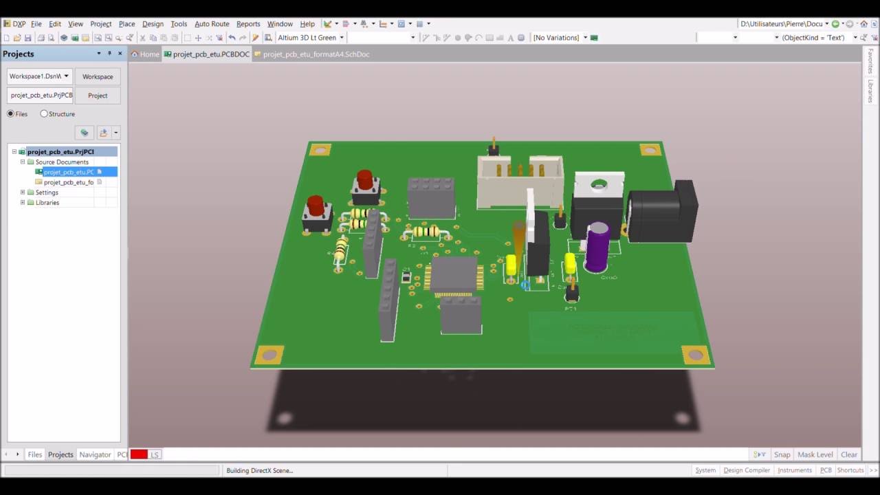
Conception De Circuits Imprimes Avec Altium Designer

Pcb Design Emsproto

Directives Et Regles De Routage Pcb Altium

Historique Du Routage Automatique Blog Altium Designer

Decouvrez Kicad Et Realisez Vos Pcb Comme Un Professionnel La Caverne De Lucan
Conception De Pcb Avec Easyeda Tutoriels Makerslide Machines

Routage D Un Pcb Avec Kicad Devenez Pro En Electronique

Cao Routage Le Secret D Un Projet Electronique Mecanique Reussi
Routage Cao D Une Carte Electronique Avec Des Signaux Rapides

Routage De Pcb 8 Choses A Savoir Sur La Conception

Routage D Un Pcb Avec Kicad Devenez Pro En Electronique

Top 10 Pcb Routing Tips For Beginners Eagle Blog

Routage D Un Pcb Avec Kicad Devenez Pro En Electronique

Le Calcul D Impedance Des Paires Differentielles Altium

Lectronique Embarque Processus De Conception Du Systeme De Mise En Page Pcb Routage Banque D Images Et Photos Libres De Droits Image
Q Tbn And9gcqgppkzzekeeob1f28j Fghppmkrby0ofulspos309erumrbgkz Usqp Cau

Routage D Un Pcb Avec Kicad Devenez Pro En Electronique

Routage D Un Pcb Avec Kicad Devenez Pro En Electronique

Routage D Un Pcb Avec Kicad Devenez Pro En Electronique
Formations Pcb Routage Electrolab
Routeur Pcb Mocn Machine De Routage De Panneau Pcb Ysvc 650 Buy Routeur Cnc Pcb Routage De Circuits Imprimes Routeur Cnc Product On Alibaba Com

Meilleures Pratiques En Matiere De Routage De Pcb En Attendant Que Le Routage Automatique Atteigne

Top 10 Pcb Routing Tips For Beginners Eagle Blog

Pcb Layout
Orbi Uliege Be Bitstream 2268 7308 3 Presentation Pdf

Conception Pcb Archivi Cadlog

Chine Le Routage De Forage Machine Cnc De Pcb Avec Quatre Broches Acheter Equipement De Forage De Routage De Forage Machine Sur Fr Made In China Com

Icad Pcb
Resoudre Les Defis Modernes Du Routage De Pcb
Conception Electronique Etude Electronique Routage Pcb Fabrication Id3
Formations Pcb Routage Electrolab
Resoudre Les Defis Modernes Du Routage De Pcb

Conception Electronique De Vos Produits Smart Eda

Pcb Design Emsproto
Formations Pcb Routage Electrolab
Formations Pcb Routage Electrolab

Lectronique Embarque Processus De Conception Du Systeme De Mise En Page Pcb Routage Banque D Images Et Photos Libres De Droits Image
Grossiste Routage Pcb Acheter Les Meilleurs Routage Pcb Lots De La Chine Routage Pcb Grossistes En Ligne Alibaba Com

Routage D Un Pcb Avec Kicad Devenez Pro En Electronique
1
Grossiste Routage Pcb Acheter Les Meilleurs Routage Pcb Lots De La Chine Routage Pcb Grossistes En Ligne Alibaba Com

Geii Eu
Cao Electronique Etude Conception Et Routage Des Pcb Altium Orcad Cadence

Etude Et Realisation De Pcb Pdf Free Download

Lectronique Embarque Processus De Conception Du Systeme De Mise En Page Pcb Routage Banque D Images Et Photos Libres De Droits Image
Formations Pcb Routage Electrolab

Pcb Design Emsproto
Assemblez Une Carte Electronique Concevez Un Objet Connecte Autonome Du Capteur A Son Antenne Openclassrooms
Formations Pcb Routage Electrolab

Pcb Design Emsproto
Formations Pcb Routage Electrolab

Pcb Design Les Differentes Phases De Conception Du Pcb Infographie


